The Hardware Ceiling: Why Physical Silicon Is Quietly Becoming AI's Most Dangerous Constraint
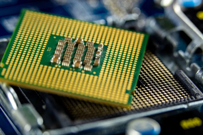
The dominant narrative inside the American AI industry follows a familiar arc: larger models, smarter architectures, more efficient training pipelines. Billions of dollars and enormous intellectual capital flow toward the software layer, toward the algorithms, the parameter counts, the inference optimization tricks. What receives comparatively little attention is the physical substrate on which all of it runs—and the degree to which that substrate is beginning to impose hard limits that no amount of clever engineering at the software layer can circumvent.
This is not a distant theoretical concern. It is an operational reality quietly reshaping deployment decisions at major cloud providers, semiconductor companies, and AI-native startups across the United States. The gap between what AI software can theoretically accomplish and what the physical silicon ecosystem can actually deliver is widening. Understanding that gap—and who is positioned to close it—may be among the most consequential questions in enterprise technology today.
Memory Bandwidth: The Bottleneck Behind the Bottleneck
When engineers discuss AI hardware constraints, the conversation frequently gravitates toward compute—raw processing power measured in teraflops or petaflops. But for many modern AI workloads, compute is no longer the primary constraint. Memory bandwidth is.
Large language models and multimodal systems require the continuous movement of enormous volumes of data between memory and processing units. The speed at which that data can travel—memory bandwidth—determines how quickly a model can generate outputs, regardless of how many compute cores sit idle waiting for information. As model sizes have scaled dramatically over the past three years, the memory systems supporting them have not kept pace at an equivalent rate.
High-bandwidth memory technologies such as HBM3 and the forthcoming HBM3E represent meaningful progress, but they are constrained by the physical realities of stacking memory dies and managing the heat generated by dense packaging. The result is a persistent architectural tension: software engineers design systems that assume memory will be fast and abundant, while hardware engineers work within physical limits that make both speed and abundance expensive to achieve simultaneously.
For enterprise buyers deploying AI inference at scale, this tension translates directly into cost and latency tradeoffs that have no clean software-side solution.
Thermal Dissipation and the Density Dilemma
Beyond memory bandwidth, thermal management has emerged as one of the less-discussed but increasingly critical constraints on next-generation AI hardware. As chip designers attempt to pack more transistors and more specialized compute units into smaller physical spaces, the heat generated per unit area increases accordingly. Removing that heat efficiently enough to sustain peak performance—without throttling clock speeds or damaging components—is becoming a genuine engineering frontier.
Data centers operated by hyperscalers such as Google, Microsoft, and Amazon have responded by investing heavily in advanced cooling infrastructure, including liquid cooling systems that circulate coolant directly across chip surfaces. These solutions are effective but expensive to build and operate. For enterprises that do not have the capital or physical infrastructure of a hyperscaler, the thermal constraints of dense AI hardware can represent a meaningful barrier to on-premises deployment.
The implications extend beyond cost. Thermal throttling—the automatic reduction in clock speed that processors employ to prevent heat-related damage—can degrade AI inference performance unpredictably. In latency-sensitive applications such as real-time fraud detection, clinical decision support, or autonomous systems, that unpredictability carries consequences that go well beyond inconvenience.
The Interconnect Problem Nobody Advertises
A third hardware constraint deserves attention that it rarely receives in mainstream technology coverage: interconnect bandwidth between chips and between nodes in a distributed system.
Modern AI workloads frequently exceed the capacity of a single accelerator. Training frontier models and, increasingly, running inference on large systems requires distributing computation across multiple chips, multiple nodes, and sometimes multiple racks. The speed and efficiency with which those components communicate with one another—the interconnect—determines whether the system performs as a coherent whole or degrades into a collection of components waiting on one another.
NVIDIA's NVLink and the broader NVSwitch fabric have established a high-bandwidth interconnect standard for GPU clusters, but they remain proprietary and expensive. Open alternatives such as CXL (Compute Express Link) are gaining traction as an industry standard, but the ecosystem around CXL is still maturing. For organizations building large-scale AI infrastructure today, interconnect choices involve navigating a landscape of competing standards, vendor lock-in risks, and performance tradeoffs that will shape their deployments for years.
The Semiconductor Supply Chain Adds Another Layer
Even if the engineering challenges surrounding memory bandwidth, thermal dissipation, and interconnects were solved tomorrow, the supply chain dynamics of advanced semiconductor manufacturing would introduce their own constraints. Advanced AI accelerators are fabricated at leading-edge nodes—primarily at TSMC facilities in Taiwan—using processes that require years of capital investment and cannot be rapidly scaled in response to demand spikes.
The US CHIPS and Science Act has directed substantial federal investment toward domestic semiconductor manufacturing, and facilities from Intel and TSMC are under construction on American soil. But advanced fabrication capacity takes years to bring online, and the specialized tooling required—particularly extreme ultraviolet lithography equipment manufactured almost exclusively by ASML in the Netherlands—remains a chokepoint that no single national policy can fully resolve in the near term.
For enterprise technology leaders making infrastructure investment decisions today, this means that the hardware they can procure is not merely a function of budget. It is a function of what the global semiconductor ecosystem can physically produce, and that supply remains constrained relative to the demand that AI adoption is generating.
Where Competitive Advantage Is Actually Being Built
Against this backdrop, a quieter form of innovation is taking shape—one that will likely define competitive positioning in enterprise AI more durably than the next incremental improvement in model architecture.
Companies investing in custom silicon—Google's TPU lineage, Amazon's Trainium and Inferentia series, Microsoft's Maia accelerator—are not simply chasing cost efficiency. They are attempting to escape the constraints imposed by general-purpose hardware by designing chips whose memory systems, thermal profiles, and interconnect architectures are optimized for specific AI workload characteristics. This approach sacrifices flexibility for performance, a tradeoff that makes sense when workloads are well-understood and high-volume.
At the startup level, a cohort of semiconductor companies—Cerebras, Groq, Tenstorrent, and others—are pursuing architectural approaches that challenge the conventional GPU paradigm more fundamentally, addressing memory and interconnect constraints through novel chip designs rather than incremental refinements of existing architectures. Not all of them will succeed, but the diversity of approaches is a reasonable indicator that the industry recognizes the depth of the problem.
For enterprise technology professionals and early adopters navigating AI infrastructure decisions, the practical implication is clear: hardware constraints are not a temporary inconvenience that software progress will eventually dissolve. They are structural features of the current technological landscape that will shape what AI systems can do, how much they cost to operate, and which organizations can deploy them effectively.
The companies that understand this—and that build their AI strategies around hardware realities rather than software aspirations—are the ones most likely to find durable advantage in the years ahead. The silicon ceiling is real. The question is who is already building toward it with clear eyes.